In today’s post, I will analyze the effect of MCPCB’s (metal core printed circuit board) through-plane thermal conductivity on the chip’s maximum temperature by using a simplified analytical thermal model, i.e. a composite slab model of three layers that consist of chip, PCB, and heat sink. The heat sink is assumed to be cooled by the air through convection.
The goal of this exercise is to see if the convective cooling requirements can be lowered by strategically lowering the conduction resistance of the PCB layer. It is assumed that the semiconductor chip of size 30mm by 30mm and power dissipation of 4 Watts can only operate below 75 degC. In this case, what type of MCPCB should be used?
The junction temperature is calculated from the model by varying both the PCB’s thermal conductivity ‘K2’ and the cooling air heat transfer coefficient ‘h4’. The results are plotted in the attached 2D graphs (Note: another way to present the results is with a 3-D surface graph by plotting the junction temperature (z-axis) vs K2(x-axis) and h4 (y-axis)).
For the assumed thermal target of 50 degC, the relationship between K2 and h4 was found by taking a horizontal slice of the 3-D surface at 50 degC. The first thing to notice is that the convective heat transfer coefficient ‘h4’ will decrease by increasing the thermal conductivity of MCPCB ‘K2’, which means less cooling power is required for the heat sink if a higher thermal conductivity MCPCB board is selected in the design. Furthermore, the most “effective” combination of K2 and h4 was found to be (K2=5 W/m-K and h4=200 W/m^2-K) for the thermal target of 50 degC, since increasing the thermal conductivity of MCPCB beyond 5 W/m-K will not reduce the convective cooling requirement significantly as the value of h4 flattens out beyond the point.Similarly, for the thermal target of 75 degC, the most “effective” combination was found to be K2=2 W/m-K and h4=100 W/m^2-K.
In conclusion, by choosing the right MCPCB, the convective cooling requirement can be significantly reduced, and every thermal target has an optimized combination of K2 and h4.
Thursday, August 18, 2011
Wednesday, August 3, 2011
Electronic Cooling - Serpentine Cooling Channel
In today's post, I will examine the application of cooling an array of semiconductor chips (3 by 10) with a serpentine cooling channel (a fluid cold plate). Similar products can be found at:
http://www.aavidthermalloy.com/solutions/liquid-cold-plates
Each semiconductor device dissipates power at 4.5W so that the total power dissipated is 135W. The inlet air is moved at 1.067 CFM at 25 degC, and it passes through the channel in 12 passes. Please see the attached graph for dimensions in mm.
Monday, August 1, 2011
Electronic Cooling - Modeling The Velocity and Temperature Distributions Inside an Electronic System
The casing design plays an important role in the thermal management of electronic chips, as the fluid dynamics inside the casing can strongly affect the chip's temperature. Fundamentally, this is a forced convection heat transfer engineering problem, and it needs to be solved by first modeling the air flow (step1) and then modeling the thermal energy (step2). In today's post I will use the Computational Fluid Dynamics (CFD) method to model the air flow and temperature distributions inside a casing that houses three units of electronic chips.
Assume a casing of size 6.25in X 4.0in X 5.0in with two internal fans (R=0.875in) is used to house three units of electronic chips that are lined up side by side (please see the graph). The casing has two end plates. The first end plate houses two internal fans that are stacked on top of each other (inlet), while the second end pate is perforated to allow the air to pass through (outlet). Each fan supplies the air at the volume flow rate of 10 ft^3/min (CFM). Each chip dissipates power at 10 Watts, and it is connected to a PCB (printed circuit board) and an aluminum heat sink. Please refer to the graph for dimensions (all dimensions are in inches).
The first step of the CFD procedure will be solving for the air flow distribution assuming,
1) no-slip boundary conditions at the solid surfaces
2) the flow is assumed to be viscous, incompressible flow (Mach number <0.3)
3) The chip dissipates heat at 10 Watts.
Material Properties
1) The PCB is a composite structure and anisotropic (i.e. the material properties are different in different axes):
Through-Plane Thermal Conductivity = 0.00847611 W/in-K
In Plane Thermal Conductivity = 2.1757 W/in-K
Density = 4.04376E-5 lbf-sec^2/in^4
Specific Heat = 146713 W-in/lbf-s-K
2) The Chip is isotropic:
Thermal Conductivity In All Directions= 0.019812 W/in-K
Density = 2.52419E-4 lbf-sec^2/in^4
Specific Heat = 147239 W-in/lbf-s-K
3) The Aluminum Heat Sink is isotropic:
Thermal Conductivity In All Directions=5.1816 W/in-K
Density = 2.53074E-4 lbf-sec^2/in^4
Specific Heat = 157054 W-in/lbf-s-K
The CFD solves for the air flow distribution, and the results are described below:
1) The first thing to notice is the formation of Eddie current in the corners of the casing. The Eddie current creates a recirculation zone that essentially "blocks" the incoming air. As a result, the air is forced to flow into the space in between the chips before it loops around them near the ends of the PCBs (Please see the animated video).
2) The chip in the center has the best flow rate among the three as the air is directly blown across its surface at high velocities on both sides - 70 to 112 in/sec.
3) The chip in the right side has good flow rate on the backside of the PCB board (40 in/sec) but not on the heat sink side (20 in/sec) as the air needs to flow around the PCB before it can reach the heat sink.
3)The chip in the left side has low flow rates on both the heat sink side (56 in/sec) and the PCB side (14 in/sec).
The second step of the CFD procedure is to solve for the temperature distribution based on the flow velocity distribution obtained in the first step. The flow is essentially advecting heat from the surfaces of the electronic parts. The results are shown below:
1) The chip in the center (coolest) is at 75 degC while its PCB is at 56 degC.
2) The chip in the right is at 101 degC, while its PCB is at 75 degC.
3) The chip in the left is at 111 degC, while its PCB is at 89 degC
Saturday, July 30, 2011
Electronic Cooling - Relationship between junction temperature and heat transfer coefficient
Thermal management is a critical issue in macro LED lighting industry since the high P-N junction temperature has several adverse effects as listed below:
1) High junction temperature can reduce the luminous efficacy (lumens/watts)
2) reduced forward voltage
3) shifted the dominant wavelength (nm). As the wavelength shifts, the color of the LED light will change accordingly. In the LED UV curing process, it is crucial to produce steady wavelengths in order to have tight control of the curing process
4) Reduced the lifetime of LED
The operating window of the LED is relatively small as it operates between the ambient (25 degC) to about 100 degC. The primary mechanism for heat transfer from the junction to the heat sink is conduction, while the removal of heat from the heat sink surface is by free convection or forced convection. It is important to keep in mind that the junction temperature will be affected by the rate-limiting step of the entire heat transfer mechanism.
A thermal model can be made with the electric circuit analogy, in which thermal resistance is modeled as a resistor, temperature is modeled as voltage source, and power consumption is modeled as current source. And the famous ohm's law states V2 = V1 + R*I, which leads to the thermal model of:
Tj = Ta + Rja * Pd
where Tj: the junction temp [degC]
Ta: the ambient temp [degC]
Rja: the overall thermal resistance from the junction to the exterior surface of the package
Pd: Power dissipated by the LED
The overall thermal resistance is the summation of:
Rja = Rjc + Rcb + Rtim + Rhs
where Rjc: thermal resistance between the junction to the ceramic substrate [C/W]
Rcb: thermal resistance between the ceramic substrate to the PCB board [C/W]
Rtim: thermal resistance for thermal interface material [C/W]
Rhs: thermal resistance of the heat sink [C/W]
Point 1 - what is thermal resistance? it is essentially Q=delT/R; where Q is [W], R is [C/W], and delT[C].
Hence, for the same value of Q, the higher the thermal resistance; the higher the temperature gradient between the two ends. It is therefore important to minimize Rja in the LED package design in order to reduce the junction temp.
Point 2 - what is the total power consumed by the LED? according to the ohm's law, it is P=I^2*R or P=I*V.
Point 3 - combining Point 1 and 2, for a given dissipated power by the LED (Pd), the delT between the junction and the ambient is the product of dissipated power and the overall thermal resistance.
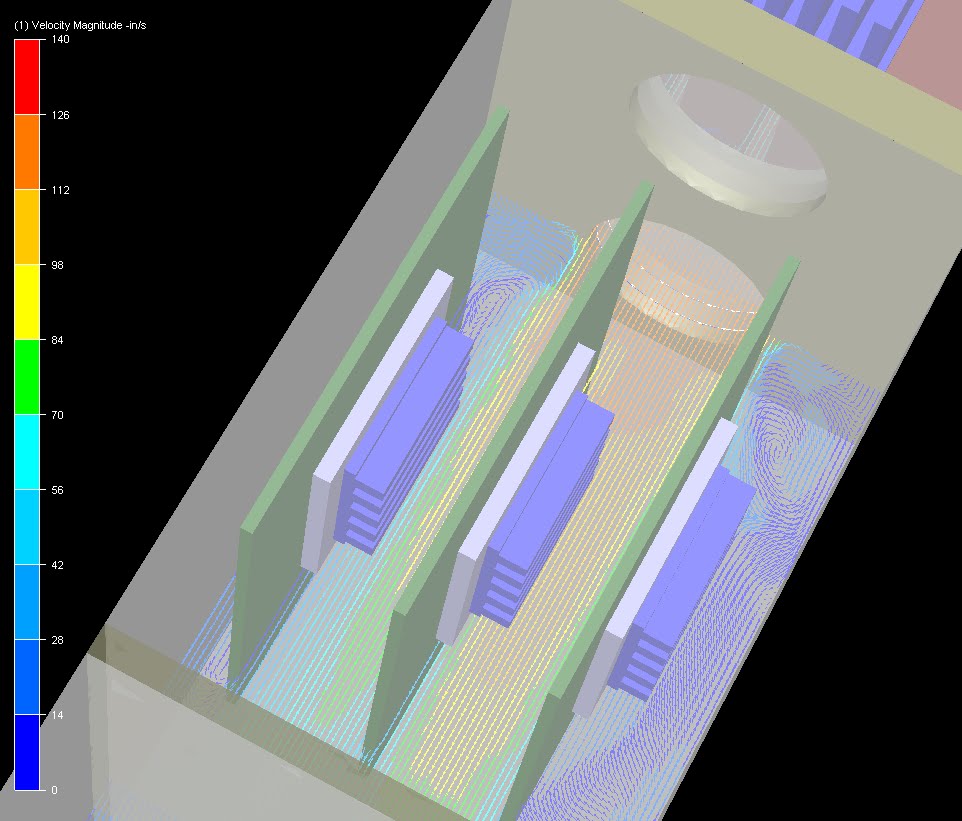
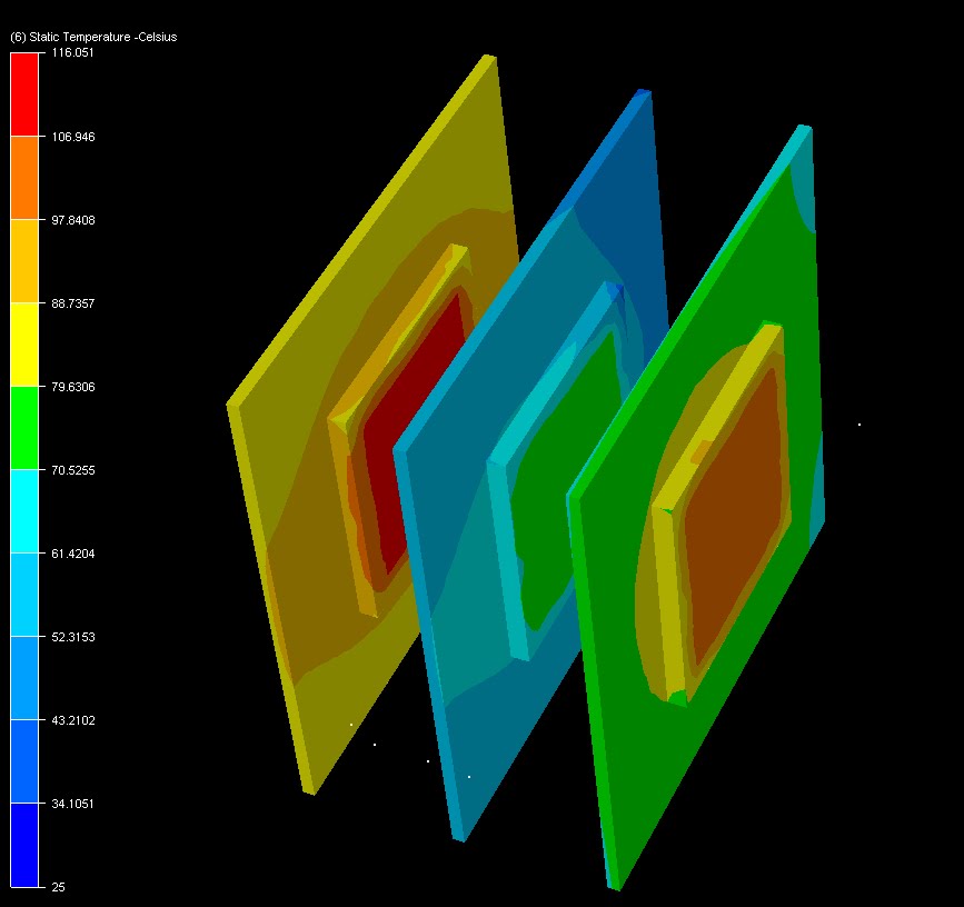
The thermal management can be dealt with from the FEA numerical simulation perspectives. And the first basic question that I asked myself is:
Q: "for a given LED package, what is the minimum heat transfer coefficient required for ensuring that the junction temperature is maintained at X?
A: Assumptions:
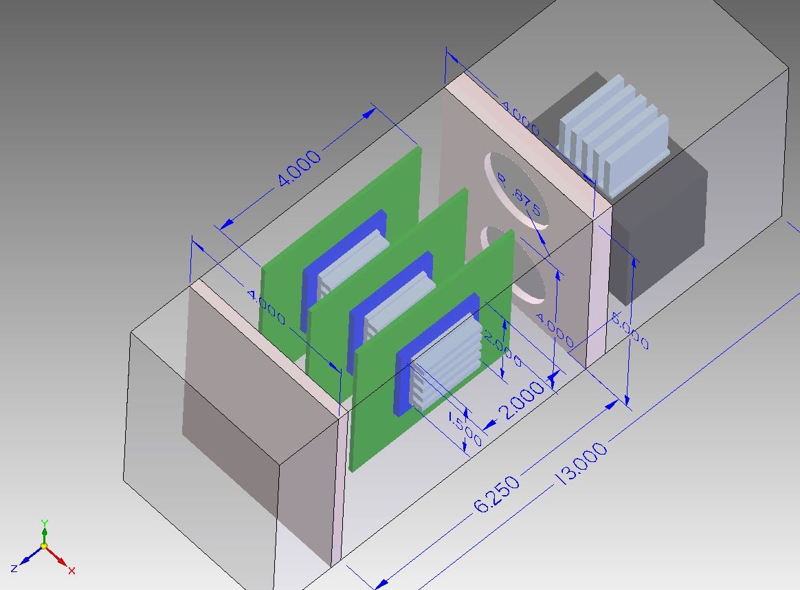
* Assume that A simplified LED package consists of 4.5W LED, a PCB board, and a conventional aluminum heat sink.
* The heat sink is 32mm by 25mm; please refer to the graph for dimensions.
* assume the surrounding air is at 30 degC.
After running the FEA model, the relationship between the junction temperature [C] and the heat transfer coefficient [(W/m^2-K] is plotted for 4.5W, 6.5W, and 8.5W LEDs as shown in the graph. The graph shows that the junction temperature will decrease rapidly with increasing the HTC value, but the rate of change of the junction temperature will gradually become flatter as it moves from the low HTC value to the higher one. This is an interesting point for the product design because it implies that the reduction in the junction temperature will become much difficult to do as the junction temperature approaches near the ambient.
Another interesting point is that the band of the curves becomes narrower as the HTC value increases. In other words, the jump in the junction temperature due to the increase in the power dissipation will decrease with increasing the HTC value. For example, at HTC=20 W/m^2-K, the jump in the junction temperature is from 72 degC to 108 degC (the difference is 36 degC) when the power increases from 4.8W to 8.5W. However, at HTC=80 W/m^2-K, the jump is from 44 degC to 60 degC (the difference is 16 degC) for the same power increase.
Subscribe to:
Posts (Atom)